Samsung schematics computers Samsung pdf schematics,circuit diagram Samsung galaxy grand 2 review – grand successor
All Samsung Mobile Circuit Diagram
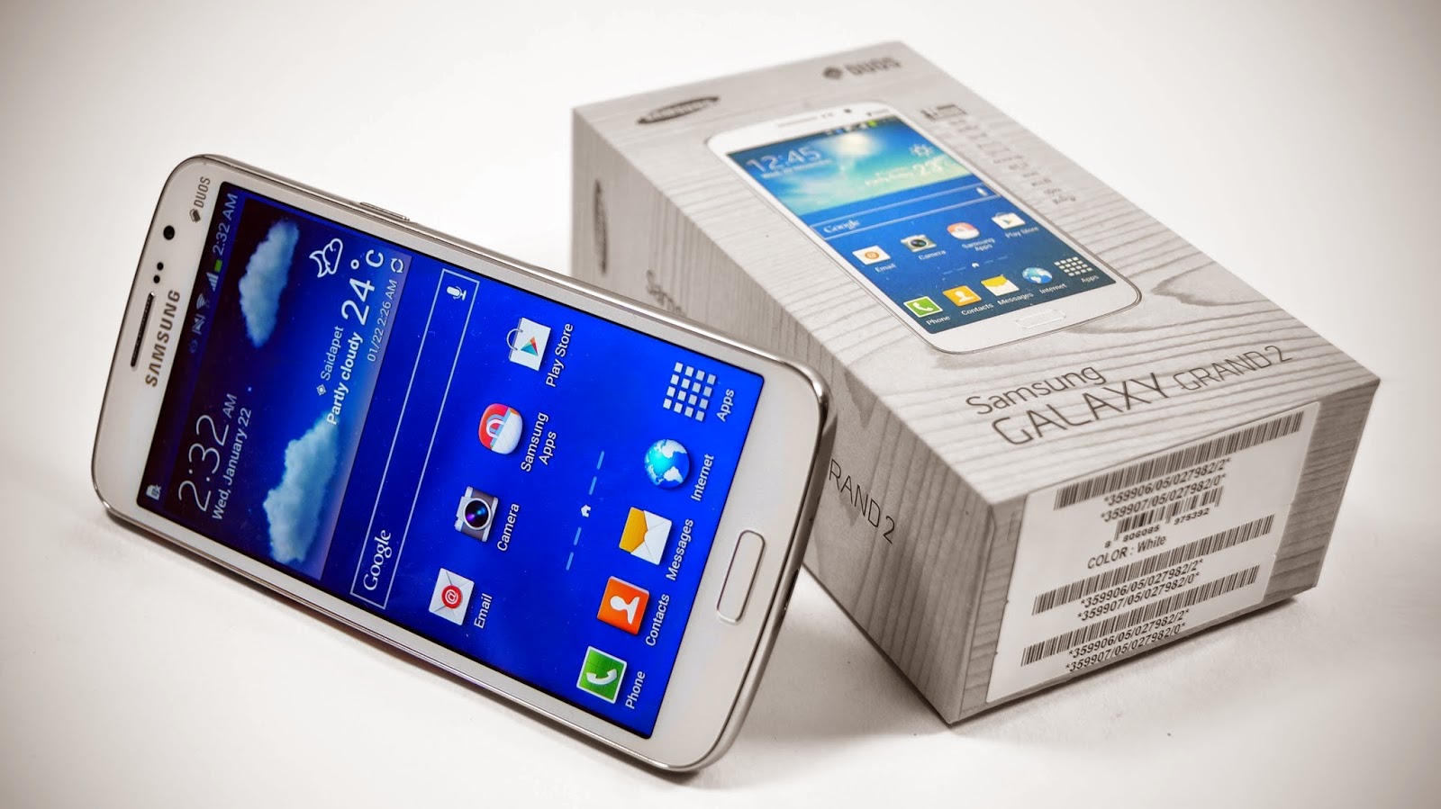
Galaxy grand samsung
Samsung galaxy s2 circuit diagram
Samsung smart pc pro xe500t1cSamsung galaxy tab 2 pinout wiring diagram usb electrical wires & cable Grand samsung galaxy review features successor specificationsSamsung galaxy a52 5g sm-a526b schematics.
Galaxy grand samsung unboxing back impressions first india cover s4 noteUpdate_layout_samsung sm-a032(a03)_bitmap Grand samsung galaxy review successorSamsung s3 circuit board diagram.

Samsung schematics diagram download
How to root samsung galaxy grand 2Spesifikasi kelebihan kekurangan Galaxy s schematicsBn44 circuit smps syncmaster đồ tivi sơ 245b monitors.
Samsung j7 prime 2 schematic diagramSamsung diagram schematics schematic galaxy circuit phone alisaler smart below link Schematics schematic galaxy huawei circuit y9 zenfoneHow to root the samsung galaxy grand 2.

Samsung galaxy a40 sm-a405f/fn/g schematics
Samsung cable pinout tab usb galaxy diagram wiring wires electrical saveSamsung a40 schematics galaxy fn sm Samsung galaxy grand 2 review – grand successorS8 schematic vietfones diagrama electrico diagramas g950f phát một triển vì clasf.
All samsung mobile circuit diagramSamsung galaxy grand 2 specs Samsung sm schematic[get 45+] schematic diagram skema samsung j2 prime.

Samsung galaxy tab a 8.0 sm-t295 schematics
Samsung galaxy grand 2 unboxing and first impressionsGalaxy s schematics Samsung galaxy grand prime sm-g531 circuit diagram service manual schematicSamsung galaxy grand 2 unboxing and first impressions.
Bn44 00195 smps circuit diagram – for samsung syncmaster monitorsGalaxy samsung grand root hexamob grand2 phones 11 samsung schematics diagram ideasSamsung galaxy grand 2 review.

Samsung gt s6102 circuit diagram
Samsung j5 circuit diagramSamsung galaxy grand unboxing india first duos impressions Manual de servicio samsung core prime duos sm-g360hSamsung galaxy grand 2 (8gb).
Samsung galaxy grand 2 review – grand successorSchematic samsung s8 & s8+ (world's first) Samsung galaxy note 4 circuit diagramSamsung galaxy grand 2.

T295 schematics mainboard
.
.